Microsoft has introduced Maia 200, its latest AI inference chip, which claims to make it cheaper and faster to run large language models. This is said to be Microsoft’s most advanced chip yet, and is built to lower the costs of generating AI tokens, which has become more challenging.
Maia 200 is made using TSMC’s 3-nanometer process and packs over 140 billion transistors. It is designed mainly for running large AI models, instead of training them. According to Microsoft, the chip offers more than 10 petaFLOPS of FP4 performance and 5 petaFLOPS at FP8, all within a 750-watt power limit.
Built for modern AI models
The chip primarily focuses on low-precision computing, which is important for running advanced AI models. It has built-in FP8 and FP4 tensor cores and a new memory system with 216GB of HBM3e memory, 7TB/s bandwidth, and 272MB of on-chip SRAM.
Microsoft says this design helps Maia 200 beat other bigger chips. The company claims it delivers three times the FP4 performance of Amazon’s third-generation Trainium and outperforms Google’s seventh-generation TPU at FP8.
Where Maia 200 will be used
Maia 200 will handle tasks inside and outside Microsoft. The chip will run the latest GPT-5.2 models from OpenAI and support services like Microsoft Foundry and Microsoft 365 Copilot. Microsoft’s Superintelligence team will also use it to create synthetic data and improve future models through reinforcement learning.
Microsoft says the chip’s design speeds up the creation and filtering of domain-specific data for synthetic data pipelines.
Networking and system-level design
Maia 200 is designed not just for computing power but also for moving data, which usually limits performance. It uses a special DMA engine narrow-precision data types, on-chip SRAM, and a custom network to keep large models supplied with data and boost token processing speed.
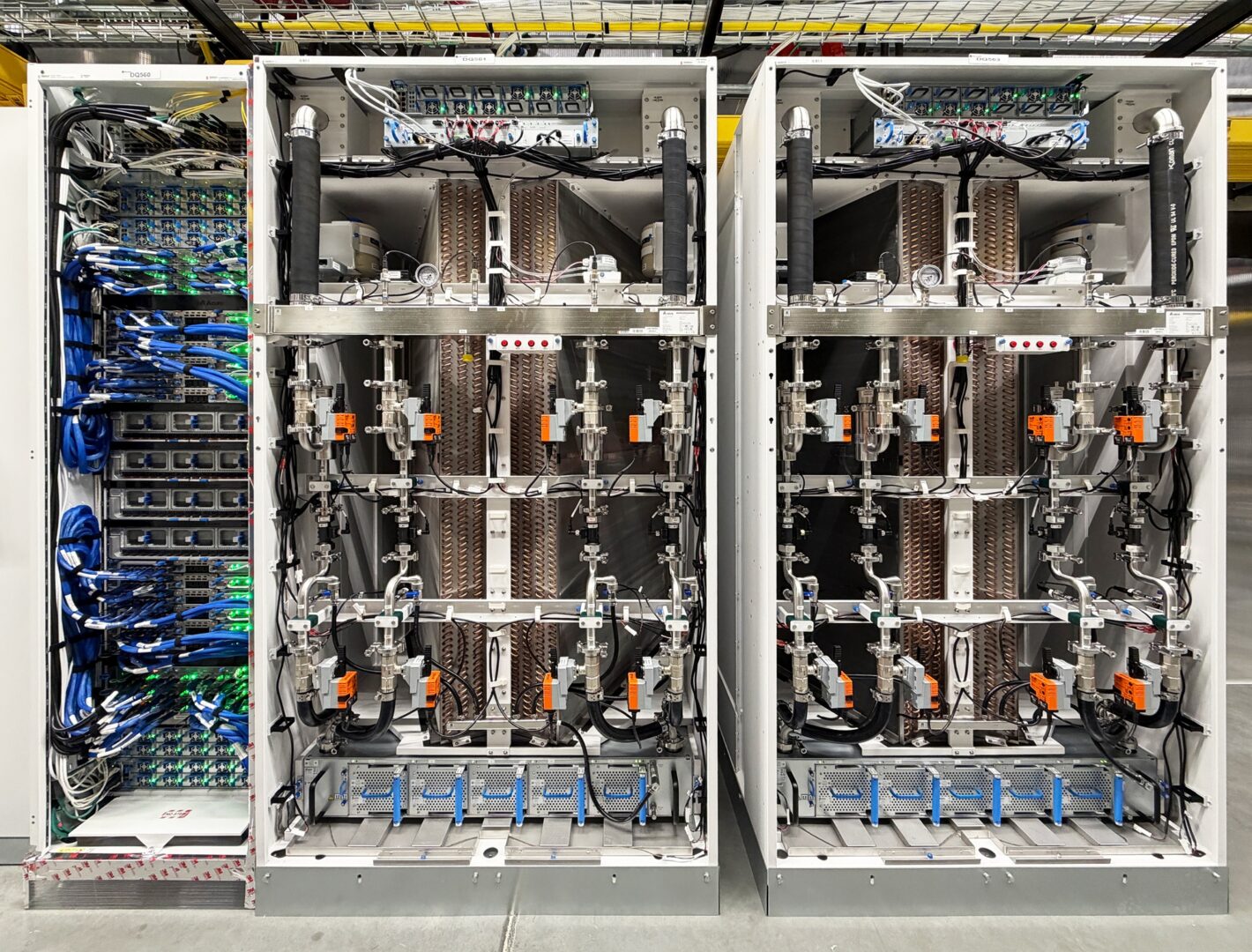
At the system level, Maia 200 uses a two-tier network based on standard Ethernet, so it does not rely on proprietary connections. Each chip offers 2.8TB/s of two-way bandwidth and can work together with up to 6,144 accelerators in a cluster.
In each tray, four Maia chips are linked directly without switches. The same communication method is used within and between racks, which helps keep performance steady and lowers network delays, power use, and total costs.
Faster path from silicon to datacenter
Microsoft says its pre-silicon validation approach helped Maia 200 reach production faster. By modeling large language models compute and communicate early on, the company able to design the chip, networking, and software together.
Maia 200 was also built with datacenter deployment in mind from the start, including early validation of backend networking and Microsoft’s second-generation liquid cooling Heat Exchanger Units. Integration with the Azure control plane enables monitoring, diagnostics, and management at both the chip and rack level.
Deployment and developer access
Maia 200 is already in use at Microsoft’s US Central data center near Des Moines, Iowa. The US West 3 region near Phoenix, Arizona will be next, with more locations planned in the future.
The chip integrates directly with Microsoft Azure, and Microsoft is previewing the Maia SDThe chip works directly with Microsoft Azure, and Microsoft is previewing the Maia SDK. This toolkit includes PyTorch support, a Triton compiler, optimized kernel libraries, low-level programming tools, and a simulator with a cost calculator.